The Ultimate Guide To Jlcpcb Design Rules Altium And Kicad Jlcpcb Design Rules For Professional Circuit Designers - Design professional schematics circuit and pcb layout on altium kicad
If you are searching about Reglas de fabricación en KiCAD | Arcos-Lab Wiki you've came to the right web. We have 35 Pics about Reglas de fabricación en KiCAD | Arcos-Lab Wiki like KiCad-DesignRules/JLCPCB/JLCPCB.kicad_dru at main · labtroll/KiCad, KiCAD-Custom-DRC-Rules-for-JLCPCB-with-Unit-Tests/JLCPCB Rules Test and also How To Import Altium PCB Board Into KiCad 7 | SaludPCB. Read more:
Reglas De Fabricación En KiCAD | Arcos-Lab Wiki
 wiki.arcoslab.org
Reglas de fabricación en KiCAD | Arcos-Lab Wiki
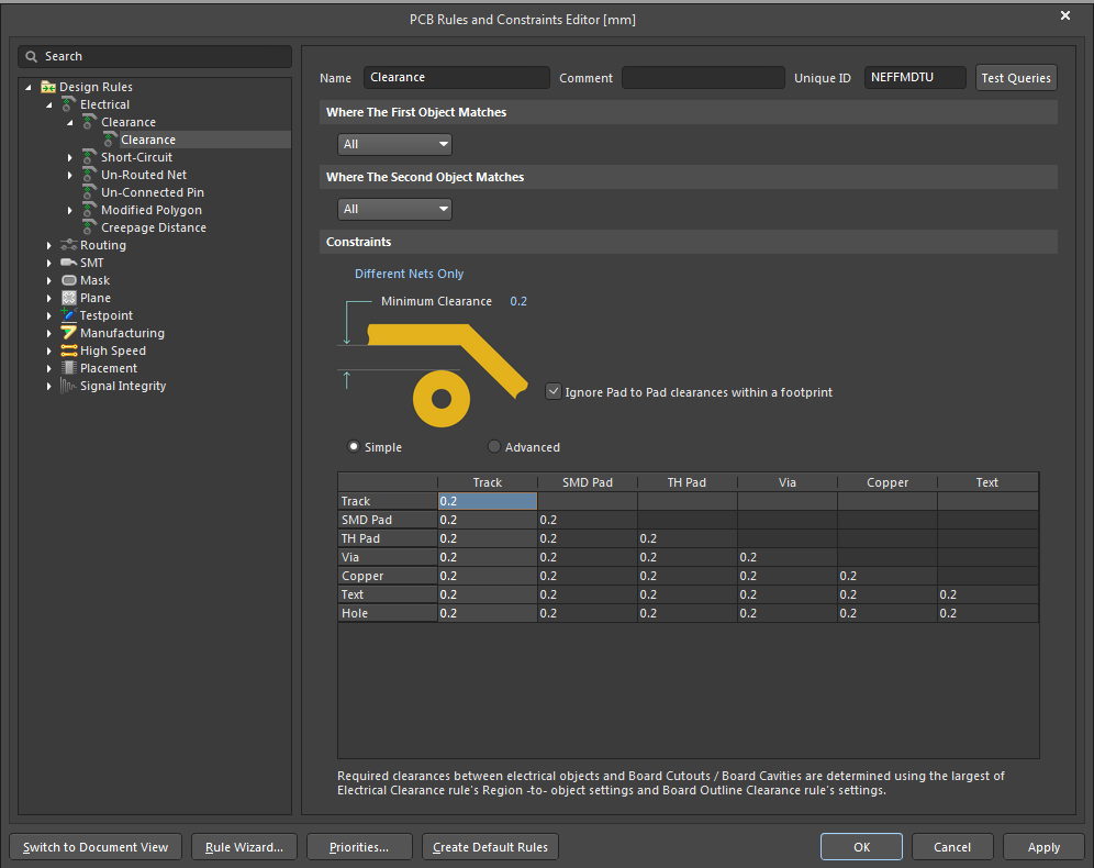
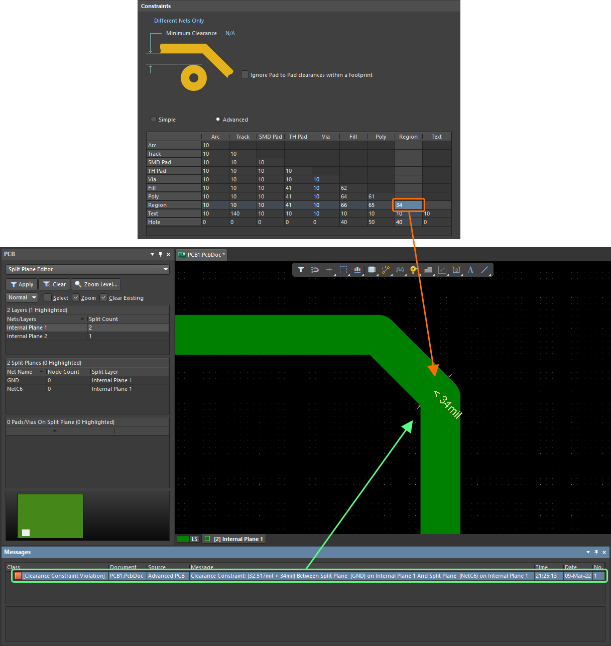
Defining Rules For A PCB | Altium App StartPage
 my.altium.com
Defining Rules for a PCB | Altium App StartPage
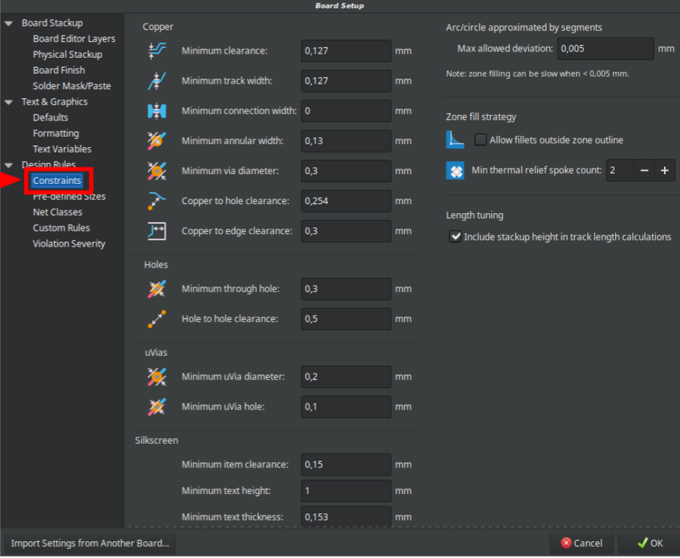
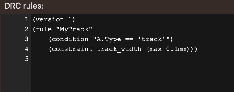
KiCad 8 Custom PCB Design Rules | SaludPCB
 saludpcb.com
KiCad 8 Custom PCB Design Rules | SaludPCB
RevK®'s Ramblings: JLCPCB And Fun Rules
 www.revk.uk
RevK®'s ramblings: JLCPCB and fun rules
How To Import Altium PCB Board Into KiCad 7 | SaludPCB
 saludpcb.com
How To Import Altium PCB Board Into KiCad 7 | SaludPCB
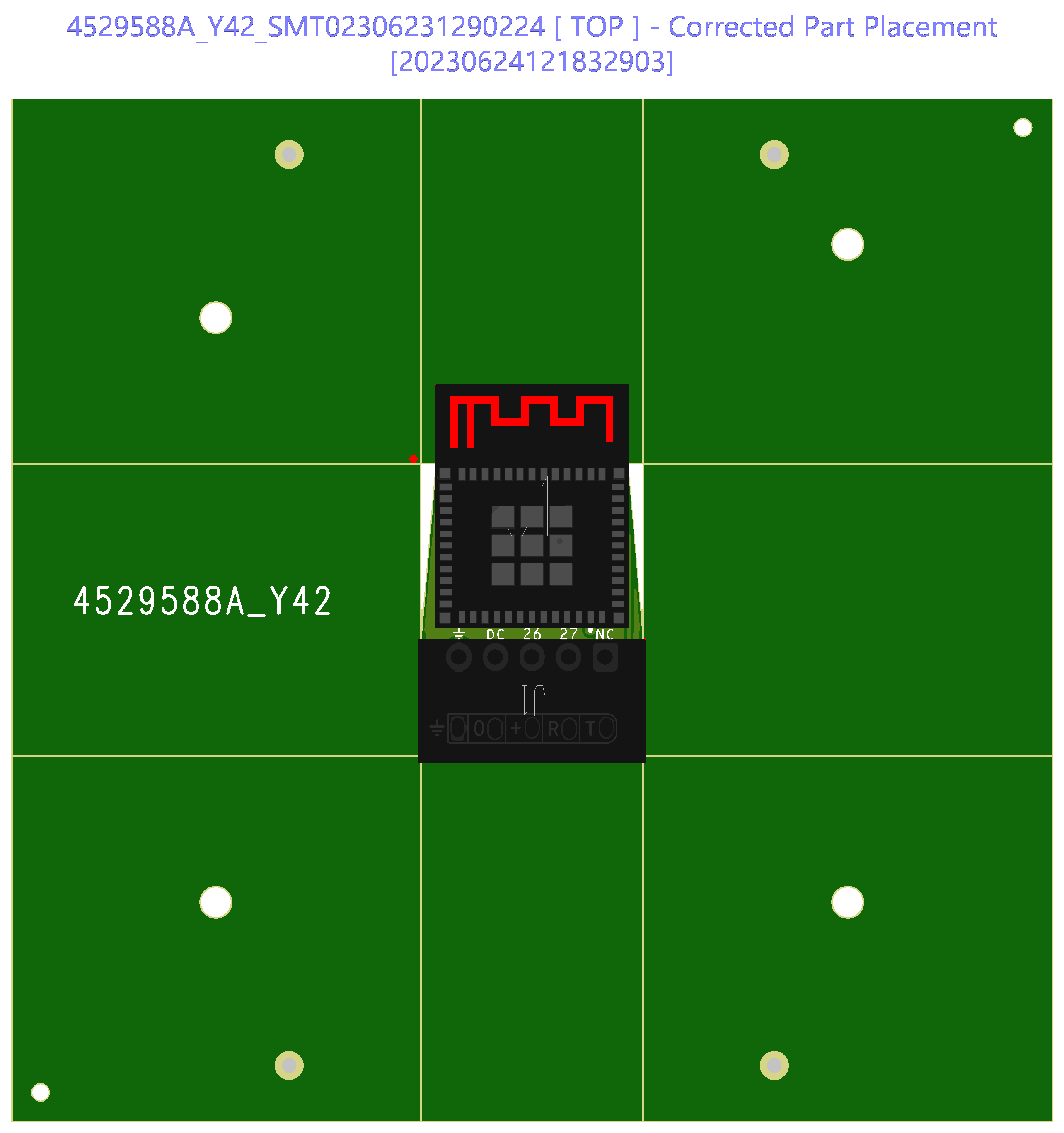
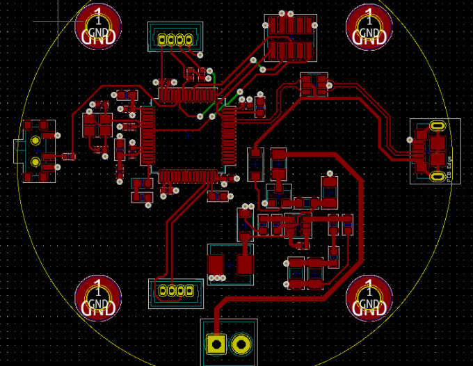
KiCad - JLCPCB, Component Placement Viewer Not Aligned. Anyone Had
 www.reddit.com
KiCad - JLCPCB, component placement viewer not aligned. Anyone had ...
Design Professional Printed Circuit Boards Using Altium, Kicad
 www.fiverr.com
Design professional printed circuit boards using altium, kicad ...
KiCad 8 Custom PCB Design Rules | SaludPCB
 saludpcb.com
KiCad 8 Custom PCB Design Rules | SaludPCB
KiCad 8 Custom PCB Design Rules | SaludPCB
 saludpcb.com
KiCad 8 Custom PCB Design Rules | SaludPCB
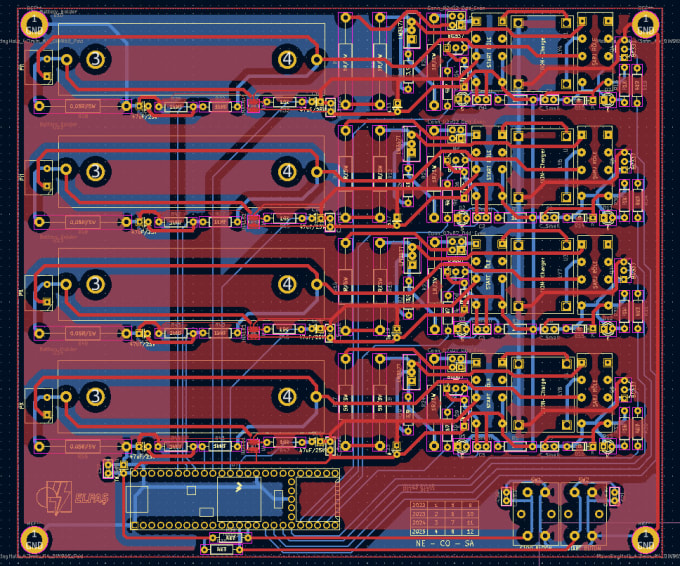
STM32 PCB Design - Complete Walkthrough - Altium Designer & JLCPCB
 www.fedevel.com
STM32 PCB Design - Complete Walkthrough - Altium Designer & JLCPCB ...
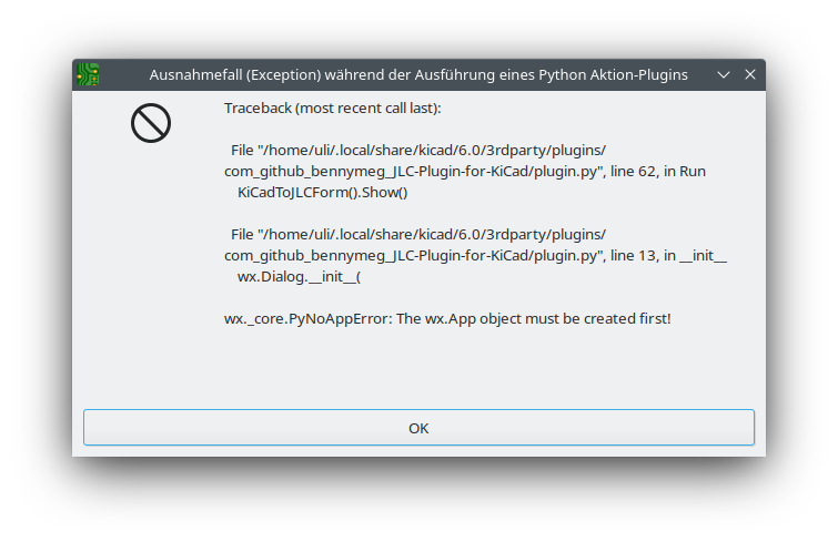
How To Fix KiCAD JLCPCB Fabrication Plugin Error: The Wx.App Object
 techoverflow.net
How to fix KiCAD JLCPCB fabrication plugin error: The wx.App object ...
Assembly Test Point Altium At Reva Forbes Blog
 storage.googleapis.com
Assembly Test Point Altium at Reva Forbes blog
Design Professional Printed Circuit Boards Using Altium, Kicad
 www.fiverr.com
Design professional printed circuit boards using altium, kicad ...
KiCad 8 Custom PCB Design Rules | SaludPCB
 saludpcb.com
KiCad 8 Custom PCB Design Rules | SaludPCB
RevK®'s Ramblings: JLCPCB And Fun Rules
 www.revk.uk
RevK®'s ramblings: JLCPCB and fun rules
BGA Pad Clearence : R/KiCad
 www.reddit.com
BGA Pad Clearence : r/KiCad
RevK®'s Ramblings: JLCPCB And Fun Rules
 www.revk.uk
RevK®'s ramblings: JLCPCB and fun rules
Develop Professional Web Application And Cloud Computing Aws By Jeremy
 www.fiverr.com
Develop professional web application and cloud computing aws by Jeremy ...
KiCAD-Custom-DRC-Rules-for-JLCPCB-with-Unit-Tests/JLCPCB Rules Test
KiCAD-Custom-DRC-Rules-for-JLCPCB-with-Unit-Tests/JLCPCB Rules Test ...
KiCad - JLCPCB, Component Placement Viewer Not Aligned. Anyone Had
 www.reddit.com
KiCad - JLCPCB, component placement viewer not aligned. Anyone had ...
Network Graph · MHI-Design/KICAD-Rules-Check-JLCPCB-2-and-4-Layers · GitHub
Network Graph · MHI-Design/KICAD-Rules-Check-JLCPCB-2-and-4-Layers · GitHub
Module 12: Design Rules - Altium
 www.yumpu.com
Module 12: Design Rules - Altium
How To Import Altium Designer PCB Board In KiCad? — RefCircuit
 refcircuit.com
How to import Altium Designer PCB board in KiCad? — RefCircuit
KiCad-DesignRules/JLCPCB/JLCPCB.kicad_dru At Main · Labtroll/KiCad
KiCad-DesignRules/JLCPCB/JLCPCB.kicad_dru at main · labtroll/KiCad ...
KiCad - JLCPCB, Component Placement Viewer Not Aligned. Anyone Had
 www.reddit.com
KiCad - JLCPCB, component placement viewer not aligned. Anyone had ...
Electronic Amplifier Circuit Guide For Beginners | Learn Basics
 jlcpcb.com
Electronic Amplifier Circuit Guide for Beginners | Learn Basics ...
RevK®'s Ramblings: JLCPCB And Fun Rules
 www.revk.uk
RevK®'s ramblings: JLCPCB and fun rules
GitHub - Wireddown/jlcpcb-kicad-templates: KiCad Templates For JLCPCB
GitHub - wireddown/jlcpcb-kicad-templates: KiCad Templates for JLCPCB
Professional PCB Layout Services | JLCPCB
 design.jlcpcb.com
Professional PCB Layout Services | JLCPCB
Faloposter.blogg.se - Kicad Altium
 faloposter.blogg.se
faloposter.blogg.se - Kicad altium
Design Professional Schematics Circuit And Pcb Layout On Altium Kicad
 www.fiverr.com
Design professional schematics circuit and pcb layout on altium kicad ...
Electrical Rule Types | Altium Designer 25 Technical Documentation
 www.altium.com
Electrical Rule Types | Altium Designer 25 Technical Documentation
Understanding And Setting Up Design Rules In KiCad
 go.pcbfabexpress.com
Understanding and Setting Up Design Rules in KiCad
Insanity 4004: JLCPCB Design Rules For Eagle
 insanity4004.blogspot.com
Insanity 4004: JLCPCB design rules for Eagle
How To Create A PCB Schematic In KiCad
.jpg?width=450&height=582&name=PCB Design Rules Handbook Cover (1).jpg) go.pcbfabexpress.com
go.pcbfabexpress.com
How to Create a PCB Schematic in KiCad
Assembly test point altium at reva forbes blog. Design professional schematics circuit and pcb layout on altium kicad. Insanity 4004: jlcpcb design rules for eagle